BB

BrainBrick.io

ESP32 Core

Complete Pinout Function & Hardware Specification Map

Lessons

BrainBrick ESP32 Master Visual Pinout Map

Hover over the board diagram to activate the precision inspection lens. Use mouse wheel or controls to adjust magnification.
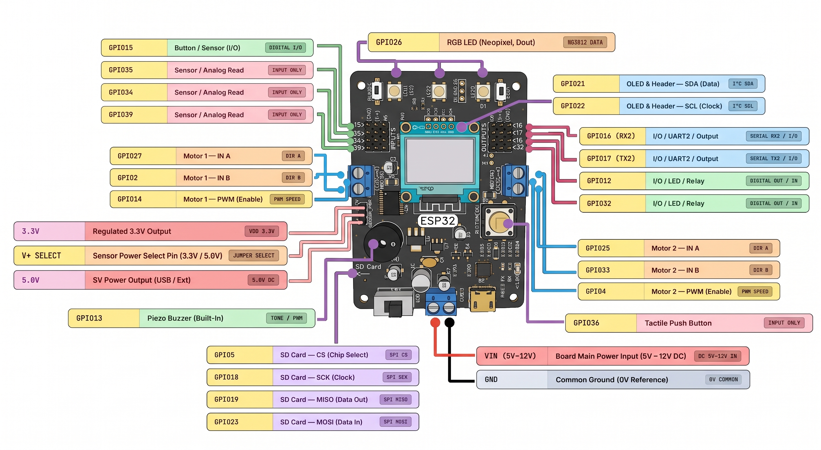
BrainBrick ESP32 Full Pinout Engineering Drawing
Hover diagram to inspect pin labels in high-definition
Showing 30 Pins / Signals
Quick Filter:

Header: OUTPUTS (Right 1×4)

GPIO 16, 17, 12, 32

User-accessible general purpose outputs. Supports digital drive (LEDs, Relays) or Hardware Serial 2 (UART2).

GPIO16 (RX2)
I/O / UART2 / Output SERIAL RX2 / I/O
GPIO17 (TX2)
I/O / UART2 / Output SERIAL TX2 / I/O
GPIO12
I/O / LED / Relay DIGITAL OUT / IN
GPIO32
I/O / LED / Relay DIGITAL OUT / IN
Adjacent Header Pins: (GND) & (V+) Max 12mA drive recommend

Header: INPUTS (Left 1×4)

GPIO 15, 35, 34, 39

Dedicated input signals for buttons, analog potentiometers, LDRs, and telemetry sensors.

GPIO15
Button / Sensor (I/O) DIGITAL I/O
GPIO35
Sensor / Analog Read INPUT ONLY
GPIO34
Sensor / Analog Read INPUT ONLY
GPIO39
Sensor / Analog Read INPUT ONLY
Adjacent Header Pins: (GND) & (V+) ADC Range: 0 to 3.3V Max

H-Bridge Dual Motor Drivers

2-Ch DC Motor Terminals

Dedicated on-board H-Bridge dual motor driver connected to blue screw terminals (Motor 1 & Motor 2).

MOTOR 1 TERMINAL (27, 2, ~14) Channel 1
GPIO27
Motor 1 — IN A DIR A
GPIO2
Motor 1 — IN B DIR B
GPIO14
Motor 1 — PWM (Enable) PWM SPEED
MOTOR 2 TERMINAL (25, 33, ~4) Channel 2
GPIO25
Motor 2 — IN A DIR A
GPIO33
Motor 2 — IN B DIR B
GPIO4
Motor 2 — PWM (Enable) PWM SPEED
PWM Resolution: ESP32 LEDC (1-16 bits) High-current H-Bridge

I²C Bus & 128×64 OLED Screen

Addr 0x3C

Internal bus driving the on-board OLED display (0.96"), simultaneously broken out to top 4-pin I2C header.

GPIO21
OLED & Header — SDA (Data) I²C SDA
GPIO22
OLED & Header — SCL (Clock) I²C SCL
Top I²C Header Pin Order: 4-Pin (JST/Dupont)
GND
3.3V
SCL (22)
SDA (21)
Display Resolution: 128×64 Monochrome SSD1306 / SH1106 Driver

MicroSD Card Slot (VSPI Bus)

Dedicated Socket

Standard SPI peripheral connection to the on-board push-push MicroSD memory socket for data logging and media.

GPIO5
SD Card — CS (Chip Select) SPI CS
GPIO18
SD Card — SCK (Clock) SPI SCK
GPIO19
SD Card — MISO (Data Out) SPI MISO
GPIO23
SD Card — MOSI (Data In) SPI MOSI
Format: FAT32 (MicroSD / TF Card) VSPI Default Channels

Built-In Peripherals (LEDs, Buzzer, Button)

Onboard Fixed

Integrated actuators and indicators directly wired to the ESP32 module on the PCB.

GPIO26
RGB LED (Neopixel, Dout) WS2812 DATA
GPIO13
Piezo Buzzer (Built-In) TONE / PWM
GPIO36
Tactile Push Button INPUT ONLY
Top Header: 5V, GND, 26 (RGB Ext) Active Peripherals

Power Rails & Hardware Strapping

System Terminals

System voltage regulation headers, ground return pads, and hardware mode buttons.

VIN (5V–12V)
Board Main Power Input (5V – 12V DC) DC 5V–12V IN
3.3V
Regulated 3.3V Output VDD 3.3V
V+ SELECT
Sensor Power Select Pin (3.3V / 5.0V) JUMPER SELECT
5.0V
5V Power Output (USB / Ext) 5.0V DC
GND
Common Ground (0V Reference) 0V COMMON
Hardware Control Buttons: Tactile Micro-switches
BOOT (GPIO0)
Hold while flashing or resetting to force ROM bootloader.
ENABLE (EN/RST)
ESP32 Hardware Reset line with pull-up. Press to restart.
Main Input: 5V to 12V DC (Screw Terminal / V+) Selectable 3.3V / 5V Sensor Rail

Critical Engineering Rules & Constraints

Input-Only Pins (34, 35, 36, 39)

These GPIOs lack output silicon driver transistors and have no internal pull-up / pull-down resistors. You cannot drive LEDs/relays from them. When connecting external switches, an external pull-up resistor (e.g. 10kΩ) is strictly required.

Analog ADC Max Voltage (3.3V)

The ESP32 internal 12-bit ADC reads values from 0 to 4095 corresponding to 0 to 3.3V. Exceeding 3.3V on any GPIO pin will permanently damage the silicon ESP32 SoC.

ADC2 Wi-Fi Restriction

ADC2 channels (GPIOs 2, 4, 12, 13, 14, 15, 25, 26, 27) cannot be used as analog inputs when Wi-Fi driver is transmitting. Notice that all BrainBrick Free INPUTS pins (34, 35, 39) are wired to ADC1, allowing flawless analog reading while streaming Wi-Fi!

Reserved Internal Flash Pins

GPIOs 6 through 11 are connected internally to the SPI flash memory chip. GPIO 0 is used for boot mode strapping. These are intentionally kept internal and not broken out to headers.

Copied to clipboard!